Fine Pitch Technology (FPT) Fine Pitch Technology (FPT)
Introduction fine pitch technology: In the ever-evolving landscape of electronic devices, the demand for smaller, lighter, and more powerful components is driving the development of advanced printed circuit board (PCB) technologies. One such innovation at the forefront is fine pitch technology, which plays a crucial role in achieving higher component density and enhanced performance. This article delves into the realm of fine pitch PCBs, shedding light on the technology, components, devices, and packages that make it possible.
Understanding Fine Pitch Technology:
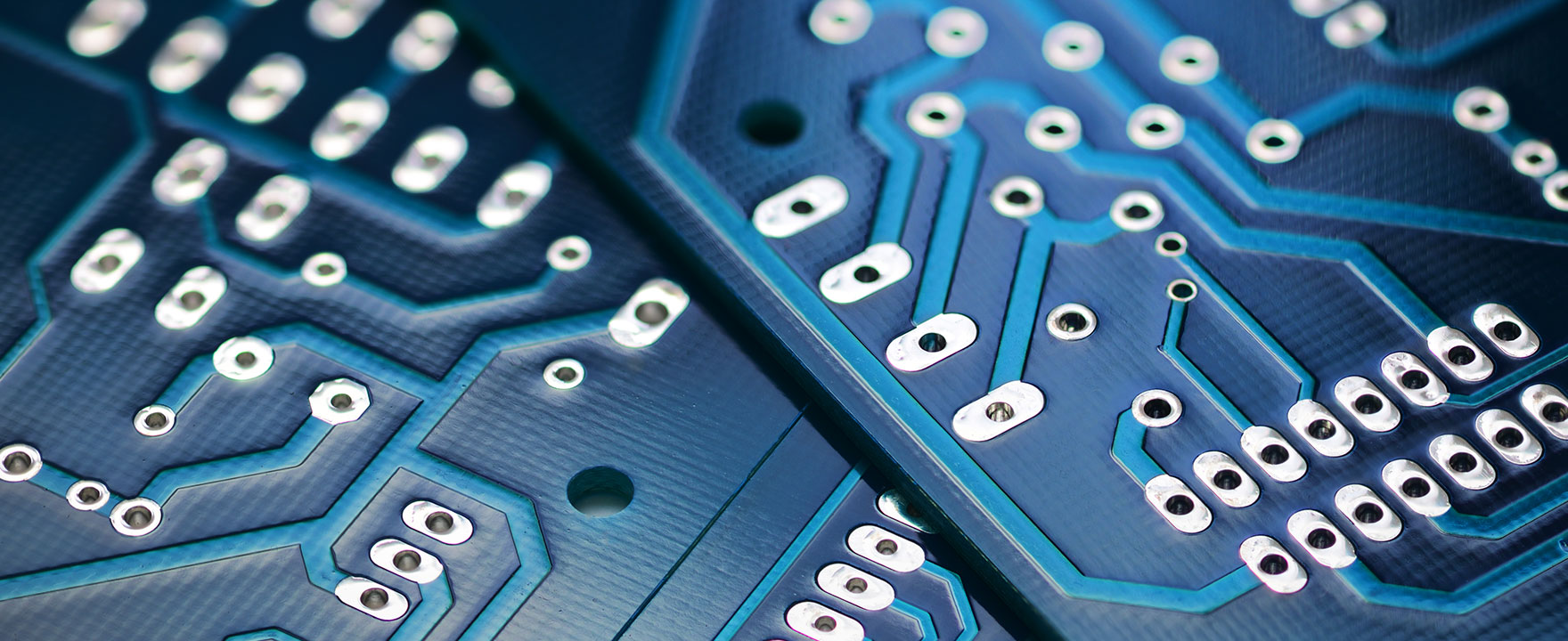
Fine pitch technology refers to the manufacturing and design techniques that enable the placement of components with a tight pitch or spacing on a PCB. The pitch is the distance between the centers of two adjacent pins or leads. In fine pitch PCBs, this distance is significantly reduced compared to traditional PCBs, allowing for a more compact layout of components.
Fine Pitch Components:
The heart of fine pitch PCBs lies in the integration of fine pitch components. These components, such as microprocessors, memory modules, and integrated circuits, have pins or leads with reduced spacing. The fine pitch design enables the placement of these components in close proximity, resulting in a higher component density on the PCB. This not only saves valuable space but also enhances the overall performance of the electronic device.
Fine Pitch Devices (FPD):
Fine pitch devices, or FPDs, are electronic devices that leverage the advantages of fine pitch technology. These devices encompass a wide range of applications, from smartphones and tablets to advanced medical equipment and aerospace systems. The use of fine pitch PCBs in FPDs allows manufacturers to create more compact and efficient devices without compromising on performance.
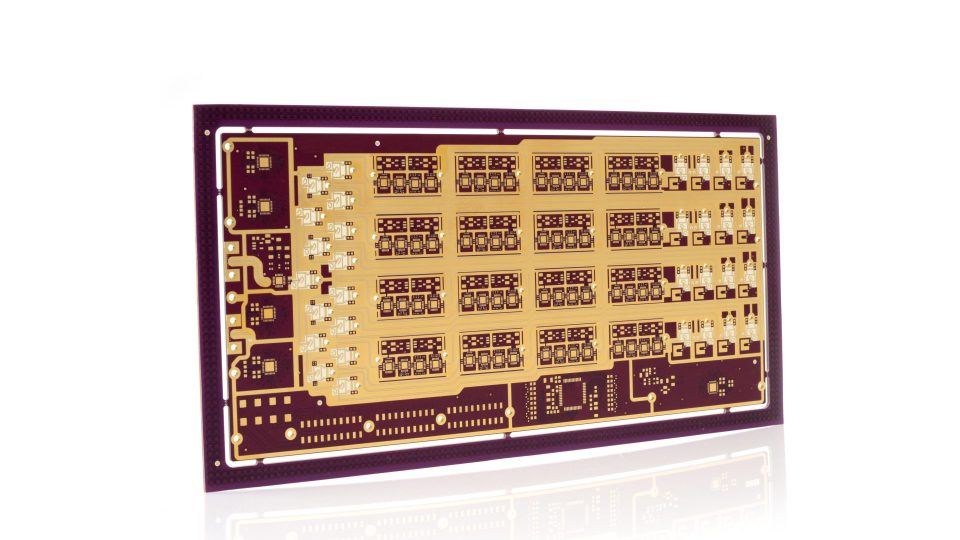
Fine Pitch Packages:
The packaging of fine pitch components is a critical aspect of ensuring reliability and functionality. Fine pitch packages are designed to accommodate the reduced spacing between pins or leads while providing robust protection and connectivity. Advanced packaging techniques, such as ball grid array (BGA) and chip-on-board (COB), are commonly employed in fine pitch PCBs to optimize the form factor and thermal performance of the package.
Benefits:
1. *Space Efficiency:* Enables the design of compact PCB layouts, making it ideal for devices where space is a premium.
2. *Enhanced Performance:* The close proximity of components on fine pitch PCBs reduces the length of signal paths, minimizing signal delay and improving overall performance.
3. *Increased Component Density:* Allows for a higher density of components on the PCB, paving the way for more powerful and feature-rich electronic devices.
Conclusion:
Fine pitch PCB technology represents a significant leap forward in the world of electronics, enabling the creation of smaller, more powerful, and feature-packed devices. As the demand for miniaturization and performance continues to rise, the role of this technology in shaping the future of electronic devices cannot be overstated. The intricate dance of fine pitch components on these advanced PCBs is propelling the electronics industry into a new era of innovation and efficiency.
ProductsDiscover products
The most ideal manufacturer for each type of product. Quality/delivery time/price/volume/reliability/technology. Please specify what is important for you.
Request a quoteCapabilitiesExplore capabilities
Not only capabilities in products but also in production locations on other continents. This allows AQC to easily switch in case of a calamity.
Explore capabilitiesDo you have any questions or want to make an appointment?Contact us
- info@aqcbv.com Send us an email
- 088-0045500 Reachable from 08.00 to 17.00 hours